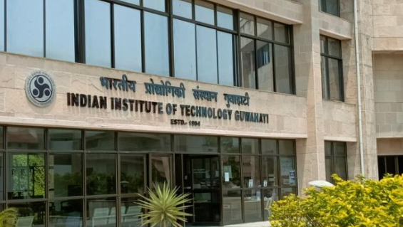
IIT Guwahati, Columbia University Developed an Optical Nanopatterning Process
Nanopatterning has come a long way thanks to scientists from the Indian Institute of Technology Guwahati (IIT Guwahati) and Columbia University in the United States. An Assistant Professor in the Department of Physics at IIT Guwahati named Dr. Rishi Maiti was very important to this study. Their results are written up in the prestigious magazine Science Advances.
What is Nanopatterning?
Nanopatterning is a complex method for making designs on materials that are very small, measured in nanometers. One nanometer is equal to one billionth of a meter. Nanoscale gadgets like advanced light detectors, solar cells, and LEDs can’t be made without this process.
The Challenge with Conventional Methods
Using electron beam lithography or other older ways to make these patterns costs a lot of money and needs special places like clean rooms. A lot of heat and plasma are often needed for these processes, which can be hard to do and cost a lot of money.
Innovative Approach with IR Laser
Dr. Maiti and his colleagues used a technique known as “optical driving” to find an easier and less expensive way to do things. With this method, a simple IR laser on a table is used to change the qualities of materials at their resonance frequency, without touching them directly.
Breakthrough in Optical Driving
The team was able to show that by “unzipping” two parallel lines on the material, they could make a nano-sized hole that could hold phonon-polaritons. These are like particles that are made when light interacts with matter, specifically when changes in the matter happen. It’s a big deal for the field that these particles can be trapped because they allow light to be focused into very small spots.
More About nanopatterning
Techniques in Nanopatterning:
- Offers high precision by focusing a beam of electrons to create nanoscale patterns.
- Uses a physical mold to shape materials at the nanoscale.
- Utilizes self-assembling polymer phases for pattern creation.
Recent Advances:
- There is a discovery that makes manipulating light at the nanoscale level easier.
- Nanopatterning is an important way to make electronics work better.
- It is an important part of making new substances that can be used in many ways.
Applications and Impact:
- Nanopatterning is an important way to make solar cells work better.
- Used to make quantum dots, which are important for new display technologies.
- Has an impact on many areas, from electronics to biology, showing how important it is in many areas.
Month: Current Affairs - May, 2024
Category: Science & Technology Current Affairs


