IISc-Samsung partner for R&D in Electrostatic Discharge Protection
Electrostatic Discharge Protection is protecting the equipment from electromagnetic waves. It is the most essential part of Electromagnetic Compatibility (EMC). Every electronic piece of equipment has to pass the EMC test to get certified as electromagnetically safe. It means it is neither affected by EM waves nor emits EM waves (that may affect other devices). Samsung has partnered with IISc to research Electrostatic Discharge Protection.
Electrostatic Discharge
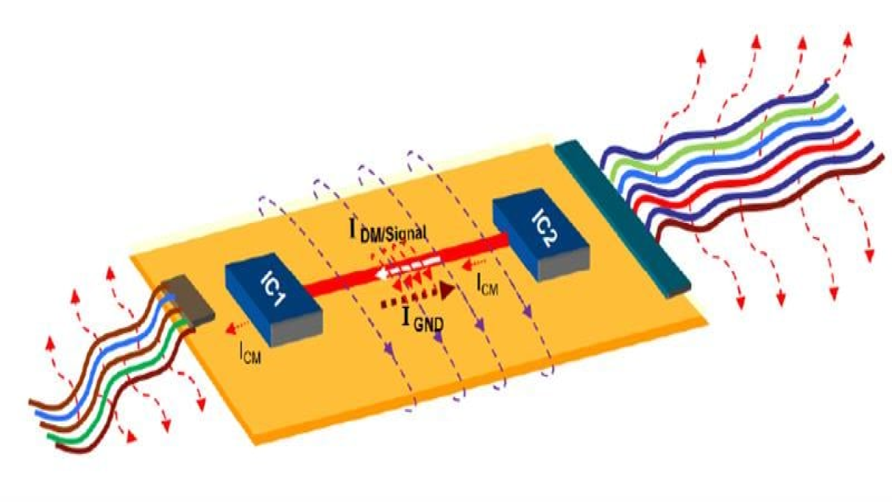
It is the sudden flow of electrons between objects. When the electrostatic discharge is high an electrical short occurs and heavy current flows between the object. This current damages the object. Where does this electron come from? While the circuit in the chip is closed and the wires are insulated, the question obviously comes where the electrons come from. These electrons are from the electromagnetic waves generated in the circuit. The transceiver circuits and high current circuits generate electromagnetic waves. The wave generates electrons.
What will the companies research upon?
IISc and Samsun will find out ways to protect the equipment from electrostatic discharge. The discharge is quite high in PCBs used in electronic devices like laptops, and cell phones. Now with nanotechnology advancing rapidly, the size of electronic components is reducing. Therefore, there is a need to place the components close to each other. This increases the challenges of Electrostatic discharge protection. The companies will work to find out solutions to protect the PCBs against electrostatic discharge.
Month: Current Affairs - February, 2023
Category: Science & Technology Current Affairs


