
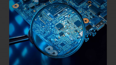
India Proposes Angstrom-Scale Semiconductor Development
Recently, a team of 30 scientists from the Indian Institute of Science (IISc) proposed the development of the world’s smallest semiconductors. This initiative aims to position India as a leader in semiconductor technology. The proposed chips will utilise two-dimensional (2D) materials like graphene and transition metal dichalcogenides (TMDs). These chips could measure one angstrom, smaller than the current production standard of three nanometres. The project seeks an investment of Rs 500 crore over five years to develop indigenous semiconductor technology.
Background
Semiconductors are essential components in electronic devices. Traditionally, they are manufactured using silicon-based technologies. Advanced nations, including the US, Japan, South Korea, and Taiwan, dominate this industry. The IISc proposal aims to shift this paradigm by exploring 2D materials that can enable chip sizes much smaller than current technologies.
Importance of 2D Materials
2D materials, such as graphene, have unique properties that can revolutionise semiconductor manufacturing. They are only a few atoms thick, allowing for unprecedented miniaturisation. The global semiconductor industry is beginning to focus on these materials as traditional scaling approaches reach their limits.
Current Global Investments
Countries worldwide are investing heavily in 2D semiconductor research. Europe has allocated over USD 1 billion. South Korea has invested around USD 300 million. Other nations, including China and Japan, are also making contributions, although their exact investments remain undisclosed.
India’s Position
India currently relies on foreign players for semiconductor production. The largest project in the country, initiated by Tata Electronics in collaboration with Taiwan’s PSMC, involves an investment of Rs 91,000 crore. This project is part of the India Semiconductor Mission and qualifies for substantial government support.
Challenges and Opportunities
Despite the promising proposal, there are challenges. The IISc project requests relatively modest funding compared to other global initiatives. There is a pressing need for India to transition from planning to execution. The global momentum in 2D semiconductor technology is rapidly building, and India risks falling behind.
Future Prospects
The IISc-led initiative could pave the way for India to establish itself as a leader in next-generation semiconductor technology. However, timely execution and substantial investment are critical. The project includes a roadmap for self-sustainability after the initial funding phase, which is essential for long-term success.
Related Posts


Month: Current Affairs - April, 2025
Category: Science & Technology Current Affairs